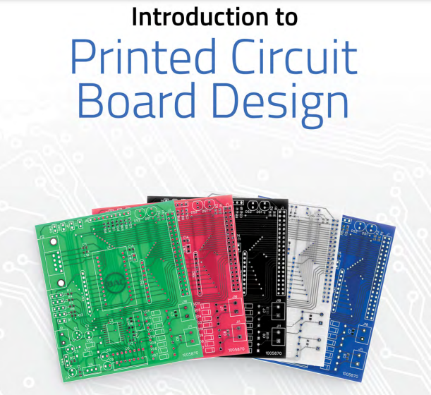

INTRODUCTION TO PRINTED CIRCUIT BOARD DESIGN https://jcubetech.ca/
About This Guide
This guide is intended for electrical engineers interested in an introduction to printed circuit
board design. It has been written to provide an overview of the design process and describes
various considerations and best practices related to printed circuit board design. The purpose
of this guide is not to provide a step-by-step tutorial of printed circuit board design, but, to
provide those with a basic background of design with some specific recommendations to ensure
desired results are achieved. For those new to printed circuit board design, it is recommended
that they first seek out training resources specific to the design software application they
intend to utilize. This information in this guide is software application agnostic and useful to
engineers with basic design expertise.
The most recent version of this guide will always be available for you
Feel free to provide feedback and change requests for this document via
email to https://jcubetech.ca/
Introduction
What happens when the initial conceptual design of a Printed Circuit Board (PCB) is complete
and its time to have the design laid out and the PCB manufactured? Many designers will
do the layout themselves while others will have a design house process the PCB layout and
fabrication data (Gerber). Many companies have their own dedicated PCB design departments
in order to shorten the learning time of their design practices. It takes an extensive amount
of knowledge to properly position hundreds of components and thousands of traces into a
design that meets an entire gamut of physical and electrical requirements. In some higher
level designs with high speed and RF capability, the design is critical and will determine if
the electronics aspect of the circuit will function. Designs must take into account that printed
circuits have resistance, inductance and capacitance. As well, the traces and dielectrics will
affect signal rise times and impedance, limiting the upper frequency.
This Introduction to Printed Circuit Board Design Guide is intended to eliminate some of the
mystery behind PCB design, enabling you to design higher quality, longer life printed circuit
boards. This guide will also provide experienced-based advice and best practices on how to
design and lay out your PCBs in a professional manner. There are many basic rules and sound
practices to follow, but there is also a lot to learn. Let’s get started!
Before Computers
Back in the pre-computer time, PCBs were designed and laid out by hand using Litho Red
Rubylith film and a swivel knife. The pattern was hand drawn and peeled off and the film
remained where you wanted copper traces. The sticky red film was used to make a silkscreen
and the traces were screened on in a positive pattern before they were etched in a tank of
ferric chloride. Later, the process evolved to use self-adhesive Bradley tapes and pads on clear
Mylar film. A tremendous number of hours were spent by designer layout specialists on a light
box cutting, placing and re-routing tracks by hand. By contrast, today very capable computers
with amazing software are utilized to layout, manage and do almost everything required to
design a PCB.

INTRODUCTION TO PRINTED CIRCUIT BOARD DESIGN https://jcubetech.ca/
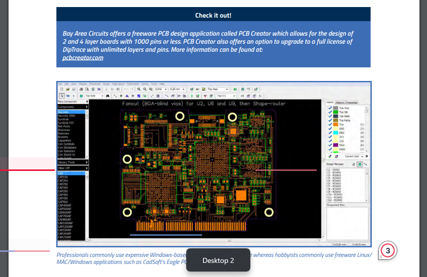
PCB Layout Software
There are many PCB design software applications available today at a wide variety of price points;
freeware to multi-server based packages. Professionals commonly use expensive Windowsbased packages such as Cadence whereas hobbyists commonly use freeware Linux/MAC/Windows
applications such as CadSoft’s Eagle PCB or Novarm’s DipTrace.
This guide will not represent any single PCB design package and the information supplied
will be universal regardless of design application. There is, however, a large benefit to using
an application which includes schematic capture and auto-routing capability.

INTRODUCTION TO PRINTED CIRCUIT BOARD DESIGN https://jcubetech.ca/
Standards
IPC (www.ipc.org) is the global trade organization that represents all aspects of the industry
including design, printed board manufacturing, and electronics assembly and test. The
primary IPC standard that covers PCB design is IPC-2221, “Generic Standard on Printed
Board Design”. IPC also provides standards to manufacturers that provide specifications for
performance and acceptability including IPC-6011, “Generic Performance Specification for
PCBs”, IPC-6012, “Qualification and Performance Specification for Rigid Printed Boards” and
IPC-A-600H, “Acceptability of Printed Circuit Boards”. These standards are useful for anyone
involved in the design, manufacture or assembly of PCBs.
The Schematic
Make sure schematics are correct and well documented with as much information as can
be included about the design. The schematic should be neat, logical and clearly organized by
area. Standard drawing practice is to have signals directly from inputs at the left to outputs
on the right. Highlight any electrically important sections. As much as possible, arrange the
schematic symbols in the same layout that the final PCB components will use. Add helpful
notes on the schematic such as drawing bypass capacitors next to the component they are
meant for, special notes for critical components and spacing requirements which will help you
or another PCB designer ensure the important parts of the project are covered. For instance:
“This pin requires a thermal relief pad to the power ground”. These notes identify areas of
concern, both mechanical and electrical, to you or the designer as to what precautions must
be incorporated. Remember to review the design. A second set of knowledgeable eyes also
helps spot the easily found mistakes.
Working Through the Board, Top Down
PCB design is always done looking from the top, down through the various layers of the board,
as if they were transparent. You will be reading text on the bottom layers as a mirror image.
INTRODUCTION TO PRINTED CIRCUIT BOARD DESIGN https://jcubetech.ca/

Traces and Spaces
There is a step by step method to determine trace and space sizes. It begins with determining
what current the trace will be carrying. If it’s a signal trace then start with the minimum you
and your PCB manufacturer are comfortable with. When laying out power or grounds then be
aware of what width traces are needed ahead of placing tracks. When running power traces
it’s wise to add a two times margin for over currents if the space is available. Remember, the
finer the traces the higher the cost due to lower production yields from the PCB manufacturer.
Next, the impedance required will affect the trace width that is selected. By determining
the dielectric constant and the impedance needed, the trace width can be calculated. Next
determine the space available and route the traces between chip pads. It is always wise to make
the traces as wide as possible to add reliability to the circuit board. It’s common for designs
to have quite a few different trace widths; some larger traces for current, some finer traces
for routing lead outs. The lower limit of the trace width will depend upon the “trace/space”
resolution that your PCB manufacturer is capable of fabricating. For example, a manufacturer
may quote a 3/3 trace/space figure which means that traces can be no less than 3 mils wide
and the spacing between traces or pads, or any part of the copper, can be no closer than 3 mils
to another copper part. Manufacturers may be capable of achieving a certain trace/spacing
but be careful not to “push the limits” with the design. For higher reliability use as large a
trace/spacing as possible until the electrical or physical design parameters call for something
smaller.
Changing a trace from large to small while moving between chip pads and then back to larger
width again is known as “necking”, or “necking down”. This allows for wider low impedance
tracks, but still maintains the ability to fan out between tight spots. However, do not reduce
traces below the PCB manufacturer’s design limitations.
Imperial and Metric
The printed circuit world operates in both the Metric system and Imperial/US Customary
units (ex. inch). As time progresses, the inch is less commonly used and use of the metric
system is growing. A simple conversion chart beside your design station can make for a great
resource. What is important is to not mistake an inch dimension for a metric one. A PCB “mil” is
equal to .001 inch or 24.5 microns. Copper weights are also expressed in microns; for example,
1 oz is equal to 1.39 mils or 35 microns. The “mil” is also called a “thou” after one thousands of
an inch. Confusing? Yes, but you will become bilingual quickly. Many designers have switched
to metric to be compatible with European and overseas PCB manufacturer requirements for
metric measurements. Make sure that any fabrication drawings state which measurement
system was utilized.

Calculating for Current
In practice, the upper trace width will be dictated by the current flowing through it combined
with the maximum temperature rise of the trace desired by the designer. Every trace will have
a calculable resistance per inch. This resistance will generate heat as current is conducted. The
trace will dissipate this heat based on surface area, air flow and the solder mask thickness. The
wider or thicker the trace, the lower the resistance, the less heat produced and the less heat
that needs to be removed. Remember the temperature rise along the trace is not linear, but
peaks in the center of a long trace due to the adjacency effect. The pads will be cooler than the
trace as the pads have larger heat dissipation.
The thickness of the copper on the PCB is nominally specified in ounces per square foot, with
½oz and 1oz copper being the most common. Thicker copper (generally up to 6 oz) can be used
for high current, high reliability designs. The calculations to determine a required track width
based on the current and the maximum temperature rise are available in many charts. A good
track width calculator program which provides results based on IPC data graphs can be found
at: circuitcalculator.com/wordpress/2006/01/31/pcb-trace-width-calculator/
As a rule of thumb, an upper limit of 20°C temperature rise in a track is a safe limit to design
around. A 10°C rise over ambient is very conservative.
Pads
Pad sizes, shapes and dimensions will depend not only upon the components being used, but
also the manufacturing process used to assemble the board. Your chosen PCB design application
should come with a set of component libraries that will define all chip and component packages.
The pad/hole ratio will affect the design by defining how large the pads will be and how small
the through holes will be; this is the ratio of the pad size to the hole size. Each manufacturer
will have their own minimum specification page, or design rules, to define what they can
manufacture. Pads for leaded components like resistors, capacitors and diodes should be
round, with around 70 mil diameter being common to fit the 35 mil hole size needed. Dual In
Line (DIL) components like integrated circuits (ICs) are better suited with oval shaped pads,
commonly 60 mils high by 90-100 mils wide. Pin 1 of the chip should always be rectangular as
a marker and with the same dimensions as the other pins. Most surface mount components
use rectangular pads, although some surface mount small outline (SO) package ICs and solder
types call for oval pads with pin 1 being rectangular

INTRODUCTION TO PRINTED CIRCUIT BOARD DESIGN https://jcubetech.ca/
Vias
Vias connect the traces from one side of the board to another by way of a hole in the board.
Vias are made with copper electrically plated holes, called Plated Through Holes (PTH). Plated
through holes allow electrical connection between different layers on the board by connecting
from top to bottom on the PCB. Microvias for High Density Interconnect (HDI) connect layers
on top of each other. The vias can also be copper filled or dielectric filled then plated flat on top
and utilized as “via in pad” technology, as well as “filled vias”. Vias can be blind or buried; blind
vias are between an outer layer and a inner layer and buried vias are between inner layers
Polygon Fill
A polygon fill which automatically fills in a selected area with copper and flows around other
pads and traces, is very useful for filling complicated ground planes. Make sure that polygon
fills are placed after all of the traces and pads have been placed. Polygon fills can either be
“solid” fills of copper, or “hatched” copper tracks in a crisscross fashion, however, solid fills
are preferred. High reliability PCBs do not use polygon fill as it creates a small gap between
all close traces and grounds. Conductive anodic filament (CAF) growth is a known reliability
problem. The small gap between traces everywhere in a polygon fill increases the chances of
creating a dendrite short. Solder mask does not stop the effect of CAF but conformal coatings
do slow it down.

Clearances
Electrical clearances are an important requirement to consider. However, there is new
information on Paschen’s law that says for curves below 350 volts, there can be no arc. All
the spacing charts are really based on environmental conditions, not voltage. Having said
that, for most circuits, clearances should be based on the amount of dirt, moisture, corrosion
and outside electrical influences, such as static arcs, that will be encountered. Even at 2 mils
spacing, a 300V signal will not arc. Add moisture or dust (which absorbs moisture), and tracking
will occur, a sort of carbon pre-short. It is always wise to allocate as much spacing as possible,
as the environment the product will be used in cannot always be anticipated.
For PCBs that use 120V and 240V AC main voltages, there are various legal and Underwriters
Laboratories (UL) requirements that need to be followed. As a rule of thumb, an absolute
minimum of 315 mils or 8mm spacing should be allowed between 120V to 240V tracks and
isolated from signal tracks with a large space or a routed slot between voltages to stop surface
arcing and tracking conductivity. The wide AC line voltage spacing is more for high voltage
spikes from the power lines as well as dust and moisture causing tracking.
For non-main voltages, the IPC standard has a set of tables that define the clearance required
for various voltages. The trace clearance will vary depending on environmental conditions,
not necessarily voltage as is stated. Tracks that are on internal layers are based on voltages,
CAF growth and carbon tracking, whereas the external surface is based more on moisture,
corrosion and dust. Some charts show changes at 3,000 m to compensate for the thinning of
the atmosphere yet Paschen curves show only a few percent difference in the arc voltage at
3,000 m. It takes 30,000 m above sea level before it makes much significant difference (20%) in
arc over voltage. Remember that below 350 volts, it is almost impossible to get a self-initiated
arc. A properly applied conformal coating will improve the effect of environmental conditions
and is often used on military specified PCBs.
Working to Grids
In the older PCB software chips and traces were laid out based on grids. With today’s very
small components, it is typical to lay out the actual parts on a relatively small grid and use
the snap to center function to connect traces to the pads. With the advanced PCB drilling and
imaging available today, there is no PCB fabrication reason to use grids, other than it makes
the PCB layout look balanced. There are multiple types of grids in most PCB drafting packages
INTRODUCTION TO PRINTED CIRCUIT BOARD DESIGN https://jcubetech.ca/
including a snap to electrical center grid and a “visible” grid. The visible grid is an optional onscreen grid of solid or dashed lines and helps in lining up components and tracks.
Another type of grid is the “component” grid. This works the same as the snap grid, but it’s
used for component movement only. This allows the designer to align components up to a
different grid but ensure that it’s made as a multiple of the snap grid.
Net connecting allows the software to know that parts must be interconnected. When a
component is moved, the software will re-route the traces to keep the tracks connected or uses
a different color identifier where crossed traces must be connected so that the connections
can be manually corrected.

INTRODUCTION TO PRINTED CIRCUIT BOARD DESIGN https://jcubetech.ca/
Component Placement & Design
The component placement is by far the most important aspect of laying out a board.
Good component placement will make the layout job easier and provide the best electrical
performance. Poor component placement can turn the routing job into a disaster, using more
layers and vias, and resulting in poor electrical performance. Every designer will have their own
method of placing components; no two circuits would ever be laid out the same. There is no
absolute correct way to place your components on the PCB but there are basic rules which will
help routing efficiency and deliver the best electrical performance for any design from a small,
simple PCB to large and complex designs.
The 10 basic steps required for laying out a complete board are as follows:
Add in your specifications; build notes, fabrication notes and date/version rev numbers
Set your snap grid, visible grid, and default track/pad sizes.
Place the components onto the board based on circuit closeness.
Divide and place your components into functional “circuit groupings” where possible.
Lay in all circuit connections into your net file.
Identify critical tracks on your circuit such as power and route them first.
Place and route each circuit grouping separately.
Route the remaining signal and power connections between circuits.
Go back over your design and do a general clean up.
Run a Design Rule Check (DRC).

These steps are by no means an all-inclusive checklist. There are many factors that determine
where components should be placed including power supply noise, current requirements and
high speed line widths and impedances, just to mention a few.
If all component positions are placed first and then you try to route everything, you can
easily run out of room and end up moving the components many times. Alternatively, if
the components are spaced out too much, you may end up with a large board that does not
make efficient use of space, with thousands of tracks and vias crisscrossing the board. The
professional way to start the layout is to get all of the components onto the screen first. If your
PCB application has a schematic package, then the quickest way to do the layout is to have
the PCB application import the schematic design and select all the components automatically.
If your PCB application does not include a schematic package, then you’ll have to select each
component from the library and place it down manually. When all the components are on the
screen, you should get a good idea if the parts will easily fit onto the size (and shape) of board
that is required. If the spacing is a tight fit, then you will have to work hard to try and keep the
component spacing tight and the trace layout as efficient as possible. The final spacing and
position of the components is critical to get all the interconnecting traces and vias within the
design space. It can sometimes take more than a few layouts to get everything positioned
without an increase in the board size.
Analyze the schematic and determine which parts of the design can be broken up into circuit
groups. When using a circuit like a complex timer, this would typically have a single input clock
line and a single output line, lots of components and connections as part of the timer. This is a

INTRODUCTION TO PRINTED CIRCUIT BOARD DESIGN https://jcubetech.ca/
classic circuit group and one that lends itself to combining all of these parts together in a separate
group. Arrange all of these parts into their own little layout off to one side for placement later as
the layout is built.
You will also need to isolate electrically sensitive parts of the design into separate groups.
Try not to mix digital and analog circuits. They need to be physically and electrically separated,
especially their grounds. The same applies to high frequency and high current circuits; do not mix
them with low frequency and low current sensitive circuits and be sure to separate the grounds.
Symmetry of the parts looks nice but is not electrically necessary in a PCB design. To speed up
the design process when using two or more identical building circuits groups, make one group
and copy the second and third one where they are needed. Start to route all the different circuit
groups separately. When the basic majority of the individual grouping routing is finished, move
and arrange the circuit groups into the rest of the design. If you don’t have anyone to check
your board over and don’t have DRC capability, use a printout of the schematic and a highlighter
pen to compare each single electrical “net” connection on the board with the schematic, net by
net. Highlight each net on the schematic as they are completed. When finished, there should
be no electrical connections left that aren’t highlighted. You can now be fairly confident that
the board is electrically correct.
Hand Routing
Routing is the process of laying down tracks to interconnect components on the board.
An electrical connection between two or more pads is known as a “net”. Keep nets as short
as possible. The longer the total track length, the greater its resistance, capacitance and
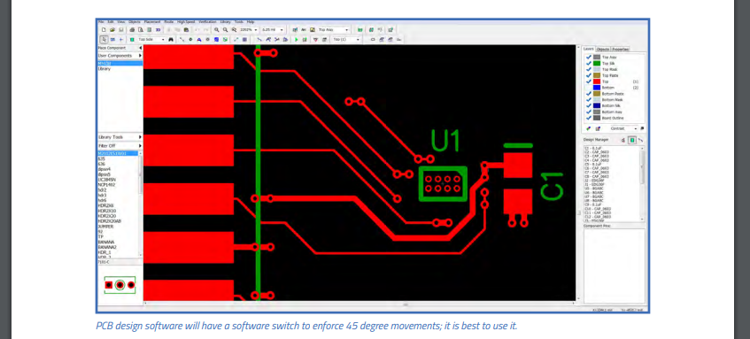
inductance, which are all undesirable factors. Tracks should only have angles of 45 degrees
which works best when running traces around the PCB.
Avoid the use of right angles and under no circumstances use an angle greater than 90 degrees
to avoid etch fluid capture in the close corners. PCB design software will have a software
switch to enforce 45 degree movements; it is best to use it. As traces are placed around the
board use 45 degree angles for turns. To run a series of traces around components don’t go
direct connection to connection unless it can be done without interference. Only use rounded
track corners with high frequency RF, signal length equalization or high voltage circuits.
Enable the center snap option (also called snap to center connection) which tells the software
to automatically locate the centers of pads and ends of tracks. As well, it places the end of
the trace inside the pad. It is important to always end a trace in the center of the pad. Don’t
make the trace just touch the pad. The snap to program and net list may not think that the
track is making electrical connection to the pad. Use a single trace and keep running it around
to connect to the desired pad. Traces tacked together end to end can sometimes be a problem
for future editing such as moving an entire component.

INTRODUCTION TO PRINTED CIRCUIT BOARD DESIGN https://jcubetech.ca/
To decide what trace width and spacing to use, the best advice is to utilize as wide a trace and
space as possible. With many PCB manufacturers using a standard trace width and space of
5/5, anything 5/5 or larger does not typically result in a price increase to manufacture the PCB.
For a PCB below 5/5, it is best to check with the PCB manufacturer as some can easily do 3/3
line width and spacing without an increase in cost.
If the power and ground tracks are deemed to be critical then lay them down first. Also, make
the power tracks as large as possible. Keep power and ground tracks running in close proximity to
each other. Don’t send them in opposite directions around the board. This lowers the inductance
of the power system and allows for effective bypassing. Split planes divide and handle two
different power supplies or digital and analog signal return grounds. Do not allow high speed
traces to flow across a gap in the power or ground planes as it will change the impedance at the
point. During clean up remove any unconnected copper fills (also called dead copper) as they just
add to the capacitance and inductance and provide more opportunities for shorts.
Cleaning Up the Design
Routing may be finished but the design isn’t quite complete. There are a few last minute
checks and finishing touches that should be performed. Check that the number of required
mounting holes on the board exist, as components can get heavy. Keep mounting holes well
clear of any components or tracks. Use the “keep out” area in the software. Allow room for any
washers and screws. Check with your PCB manufacturer to determine whether they charge
extra for above a certain number of different hole sizes. If so, simplify the design by minimizing
the number of hole sizes.
Double check for correct hole sizes on all the components and add 4-5 mils per side for
proper solder flow. Nothing is more annoying than receiving a perfectly laid out PCB from the
manufacturer only to find that a component won’t fit in the holes!
Ensure that all vias have the correct size pad. For example, the manufacturer will state that the
pad should be 12 mils above finished hole size. If the pad is too small in relation to the finished
through via, it can cause breakouts in the via pad. The hole, if shifted slightly, can be outside of
the pad. Most manufacturers will run a DRC on the design prior to fabrication and refuse the
job if the pad is not big enough. Check that there is adequate physical distance between all the
components. Watch out for components with exposed metal that can make electrical contact
by bending or thermal growth with other components or exposed tracks and pads.
Teardrops are a nice smoothing out of the junction between the track and the pad, but studies
have shown it does not give a more robust or reliable trace to pad interface. It is therefore, not
necessary to use them.
Single-Sided Layout
Single-sided PCBs cost less than double-sided. Designing the circuit as a single-sided circuit
can greatly reduce the cost of the board. Most of today’s consumer items like TVs and DVD
players, all use low cost single-sided boards. More features and components can be added to
a single-sided board with the addition of jumpers. Jumpers can be a bent wire soldered in, a
pre-bent automatic inserted wire or even silver traces silk-screened over top a dielectric layer.
If building a single-sided circuit that will be assembled with automatic machines, it will cost
less to use as many jumpers as needed, opposed to switching to a double-sided design.
However, with SMT components, a double-sided design may be less cost overall. If the design
INTRODUCTION TO PRINTED CIRCUIT BOARD DESIGN https://jcubetech.ca/
complicated component placement becomes more critical. Do not make all the components
nice and neatly aligned. Place the components so that they give the shortest and most efficient
trace routing possible. Cost and size of the circuit as well as the technology level will determine
if the design needs to be single-sided or increased to double-sided. With experience, you will be
able to determine whether a single-sided board is an option before you even begin the design
Double-Sided Layout
Double-sided PCBs allow for more components and tighter routing. Designs that were next
to impossible on a single-sided board are simpler when an additional layer is added. Doublesided design lends itself to having one side with traces running mostly in one direction and the
other side 90 degrees different. This allows you to easily drop a via down and head in a different
direction across the board. Careful component placement with efficient building block routing is
critical for a neat low via count layout. Many basic auto routers work in this way. Sometimes it
works well and other times a hand layout is better. Double-sided design can also give the chance
to make use of good ground and power plane techniques which is required for high frequency
designs. Assembling components on both sides of a PCB can have many benefits such as the
reduction of board size. Be sure to involve your PCB assembler in discussions during the layout
of the board. There are many things that can and can’t be done with double-sided loading
Silkscreen
The silkscreen layer is also known as component overlay or component identification. It is a
white epoxy layer on the top or bottom of the board that identifies the component outlines,
designators (such as C1, R1, etc) and any other important text. The epoxy ink is applied to the
board using a silk screening process or a special ink jet printer. White is the standard color but
other colors are available upon request. When laying out the component footprints, ensure
that a component overlay is added that reflects the actual size of the component on a separate
layer. This way you will be able to tell at a glance how close you can physically position the
components. Ensure that all polarized components are marked and that pin 1 is identified. The
silkscreen layer will be the most inaccurately aligned of all the layers, so don’t rely on it for
any positional accuracy. Ensure that no part of the silkscreen overlaps a bare pad. Check with
the PCB manufacturer for specifications as most limit the width of the silk screening text to
a minimum of 10 mils wide. As a general rule, don’t put component values on the silkscreen;
just the component designator.
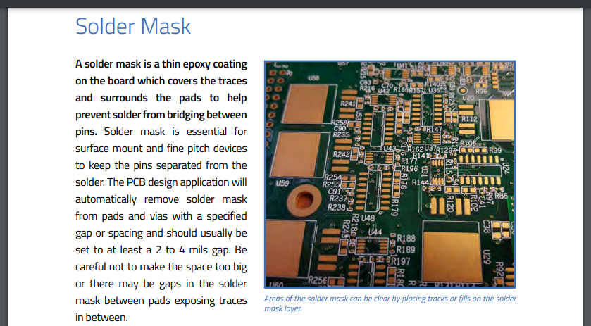
The solder mask is usually displayed in the PCB design application as a negative image, just like
the power plane. Areas of the solder mask can be clear by placing tracks or fills on the solder mask
layer. Solder masks are applied by three very different manufacturing methods; silkscreen, photo
imageable and ink jet. Photo imageable masks provide better resolution and alignment and are
preferred over the older silkscreen method but most manufacturers are moving towards the new
faster, lower cost, ink jet solder mask application. Solder masks come in many different colors but
the standard color is semi-gloss light green, typically Taiyo 4000bn Ink. On most boards, the solder
mask is laid directly over the bare copper tracks. This is known as solder mask over bare copper, or
SMOBC. Small vias can be covered or filled with solder mask; this is known as tenting or via fill. The
via is separately filled with a silkscreen of the epoxy solder mask. The filled vias are useful for close
tolerance designs to prevent solder from flowing through or into vias.
Mechanical Fabrication Layer
The mechanical fabrication layer is used to provide an outline for the board and other
manufacturing instructions. It is used to communicate the specifications to the PCB
manufacturer, as well as tolerances that the PCB manufacturer needs to work towards.
Keep Out Area
The keep out layer generally defines areas on your board where auto or manually routed
traces or components are unwanted. This can include clearance areas around mounting hole
pads or high voltage components, as examples.
Layer Alignment

INTRODUCTION TO PRINTED CIRCUIT BOARD DESIGN https://jcubetech.ca/
When the PCB manufacturer makes the board there will be alignment tolerances on the
artwork film for each layer. This includes track, plane, silkscreen, solder mask and drilling.
If there isn’t an allowance for this in the design and the tolerances are too fine, the design
may not work out as planned. Consult the manufacturer for what alignment tolerances can be
achieved – and also what alignment tolerance you are paying for!

Net List
A net list is essentially a list of connections (“nets”) which correspond to the schematic. It
also contains the list of components, component designators, component footprints and other
information related to the schematic. The net list file will be generated by the schematic package.
Generating a net list is also called “schematic capture”. The PCB design application can then import
this net list file. It can automatically load all the required components onto the blank board and can
also assign a “net” name to each of the component pins. With nets assigned to the PCB components
it is now possible to auto route, perform design rule checking (DRCs) and display component
connectivity. This is the fundamental advantage with modern schematic and PCB CAD packages.
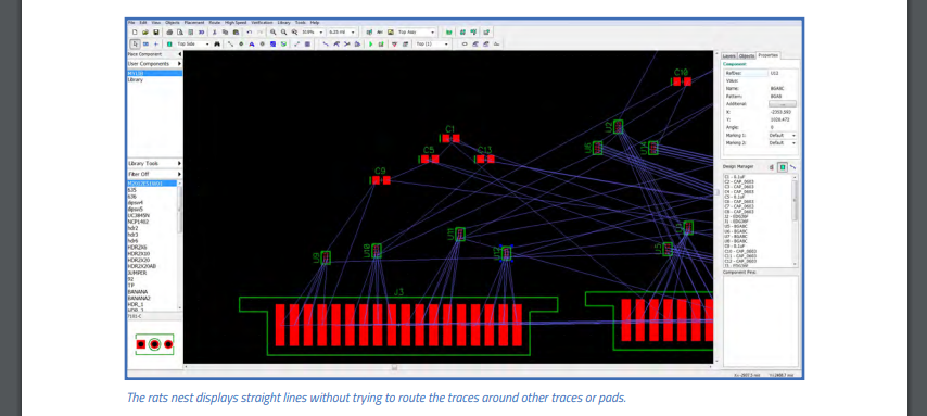
Rats Nest Display
The “rats nest” is a straight line display, connecting pad to pad, directly from the net list
generated from the schematic. The rats nest displays straight lines without trying to route
the traces around other traces or pads. As you become more skilled with routing you can grab
a single rats nest line and start to run it around other traces or pads, as well as move up and
down between layers with vias. The act of component placement will be made considerably
easier by having the rats nest display enabled. To do so, enter the schematic drawing and
import a net list which enables you to then generate a rats nest. For large designs, a rats nest
display is essential to enable you to see where traces must go, which in turn, makes routing
easier. After the components have been initially laid out enable the rats nest which will appear
as a huge and complicated random maze of lines, hence the name, “rats nest”. The rats nest
may look very confusing at first glance. However, when each component is moved, the rat nest
lines will automatically move with them allowing placement to be adjusted to get the best
fit. The rats nest allows you to see which components are connected to each other without
having to constantly refer back to the schematic and check the cross reference component
designators. You will get used to using the rats nest feature even on simple boards as it allows
you to quickly see where each trace must connect. The rats nest lines will slowly disappear as
you route and convert them to traces between components and layers. The design will get less
complicated enabling you to look for trace routes for the more difficult traces.
Design Rule Checking
Design Rule Checking (DRC) allows the PCB design software to automatically check the PCB
design for connectivity, clearance, and other manufacturing errors as specified in the DRC
file. With large and complex PCBs it is practically impossible to manually check a PCB design.
The DRC process is an absolutely essential step in professional PCB design. A proper DRC will
look at circuit connectivity as it checks that every trace on the board matches the net list of the
schematic. The DRC will look at all copper areas for proper electrical clearance between tracks,
pads, and components. The DRC will also compare manufacturing tolerances like minimum &
maximum hole sizes, track widths, via widths, thermal relief sizes, and short circuits.
A complete DRC is usually performed after the PCB design has been finished. Some software
applications, however, have the ability to perform “as you work” DRC rule checking. Example:
The design application will indicate when the connection of a trace to a pad is incorrect as per
the schematic net list, or if it violates a set clearance between trace and pad.

INTRODUCTION TO PRINTED CIRCUIT BOARD DESIGN https://jcubetech.ca/

Forward and Back Annotation
Forward annotation is when changes are made to an existing PCB layout via the net list
schematic editor. The software will use the schematic net list and component designators
and import them into the PCB design, making any needed changes. Some software packages
will also automatically remove old PCB traces that are no longer connected in real time. If the
schematic is updated, then the change must be forward annotated into the PCB design. Back
annotation occurs when one of the component designators or chip pin number on the PCB is
changed and then automatically updated back into the net list schematic. More advanced back
annotation features in some software allow for the swap of gates on chips and perform other
electrical changes.
Multi-Layer Layout
A multi-layer PCB is more expensive
and more difficult to manufacture than
a single or double-sided board, but it
opens up a large area for trace routing
especially with higher density chips and
BGA to route power and signal tracks. By
placing the signal traces on the inside of
the board you can increase the density
of the components on a given size board.
Deciding when to switch from a doublesided to a multi-layer design is influenced
by many decisions; board size, routing
density trace widths and pin out pitch.
Multi-layer boards mostly come in an
even number of layers with 4, 6, and 8
layers being the most common. Today’s
complex circuits require up to 32 layers
and are considered very specialized. Technically, you can design/order an odd number of layers,
such as a 3-layer board for instance, but the cost would be comparable to a 4-layer board so an odd
number of layers doesn’t typically save money. In a multi-layer design one layer will be dedicated to a
power plane, a second layer dedicated to a ground plane and two layers or more for trace layers which
typically run at 90 degrees to each other to ease via routing of the traces between layers. Power layers
are almost always in the middle of the board, with the multiple ground layers closer to the outside.
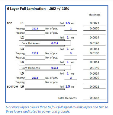
If power and ground planes are required due to high frequency, look to increase from 4 to 6 layers.
6 or more layers allows three to four full signal routing layers and two to three layers dedicated to
power and grounds.
Multi-layer and even double-sided layouts, allow for the use of different types of vias to improve
routing density. There are many types of vias; standard, blind, buried, micro and back drilled vias are
all examples. Standard through hole vias go through the whole board and can connect from the top
to the bottom, connecting to inner layers if required. There can be wasted space on layers which are
not connected but many times this is less expensive than utilizing blind or buried vias. Blind vias go
from the outside surface through layers but stop somewhere inside the board and the via does not
protrude through to the other side of the board. Blind vias are more expensive because they either
involve multiple lamination cycles by the manufacturer or require expensive equipment, like a laser
drill or special CNC drill with layer sensing technology. Buried vias are an inner board connection

INTRODUCTION TO PRINTED CIRCUIT BOARD DESIGN https://jcubetech.ca/
between two or more inner layers with no hole being visible on the outside of the board. Buried vias
can require sequential lamination on some builds if the via starts or stops on an odd layer, therefore,
incurring increased costs. Blind and buried vias are very useful and almost mandatory for very high
density designs like those involving Ball Grid Array (BGA) components. Micro vias are laser drilled and
typically only connect one layer to another and are very small at 2-4 mils in diameter. Back drilled vias
are a normal via but partially drilled to limit impedance by reducing the plated center of the via; one
side is partially drilled to limit the number of inner layer connections and plating hole length.
Power and Ground Planes
It is standard design practice to use “power and ground planes” to distribute power and
return grounds throughout the design. Using power and ground planes can drastically reduce
the power wiring inductance, electrical noise imposed on the power lines and lower impedance
to the components, which is critical for high speed digital design.
A power or ground plane is essentially one solid copper layer of board dedicated to either the
ground or power signals. Power planes are best in the middle layers of the board, usually on
the layers closest to the outer surfaces. On a 4-layer board with complex power requirements
it is typical to use one layer as the ground plane and another layer for the various positive and
negative power tracks. The ground plane is usually the signal return point and more important
than a power plane. Most PCB design applications use reversed plane layers that are laid out
opposite the other normal tracking layers. On a normal trace layer the board starts as blank
and as traces are laid they will become the actual copper traces. However, on a power/ground
plane the board starts as covered copper. Laying down traces on a power/ground plane actually
removes the copper.
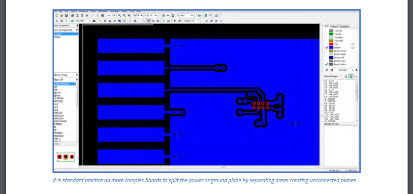
A single power/ground plane will not have any spaces or empty areas but will just be one
solid layer of copper with clearance holes in the copper plane for the through via. It is
standard practice on more complex boards to split the power or ground plane by separating
areas creating unconnected planes. This may be done to separate an analog and a digital
ground to reduce the amount of digital ground noise which is coupled into the more sensitive
analog circuitry. Be careful not to cause a power or ground loop on the board by accidentally
connecting the opposite halves of the plane on one side of the board to the other side. As a
good practice, you should place .020 to .040 wide traces (empty area) completely around the
outer edge of the power/ground plane to ensure that the power/ground planes do not extend
right to the edge of the board and allow a bare FR4 area for final routing
Grounding
Grounding is very important for the correct operation of many circuits. Good or poor
grounding techniques can make or break a design creating oscillations within the circuit.
Use as much copper as possible for the grounds, as the more copper in the ground path the
lower the impedance. Use fills and ground planes where possible. Always dedicate one of
the closest planes to the top layers to ground on multi-layer boards. Run separate ground
paths for critical parts of the circuit back to the main filter capacitors. This is known as central
grounding because the ground tracks all run out from a central point. Separate ground planes
keep current and noise of one component from affecting other components.

INTRODUCTION TO PRINTED CIRCUIT BOARD DESIGN https://jcubetech.ca/
Capacitor Bypassing
Active components in the circuit which draw significant switching current should always
be bypassed with closely positioned capacitors to “smooth” out the power trace going to a
particular device. A typical bypass capacitor is 100nF for general purpose use and mid frequency,
10nF or 1nF for higher frequencies, and 1uF or 10uF for low frequencies. It’s also possible to
have two or three different value capacitors in parallel to suppress different frequencies in the
power line. Proper bypassing has one single capacitor at each noisy gate or power supply to
a chip. It is not uncommon for a large design to have hundreds of bypass capacitors. Special
low Equivalent Series Resistance (ESR) capacitors are used on critical designs such as high
noise switch mode power supplies. With a large quantity of dense high speed surface mount
devices packed onto a PCB there is little room for the many bypass capacitors required. Often,
they cannot be placed close enough to the device power pins to be effective. Ball Grid Array
(BGA) devices are one such component that benefit from having the bypass capacitors on
the bottom of the board. It is common to design double sided loaded boards with bypass
capacitors mounted on the back so that the bypass capacitor is as close to the physical device
power pin as possible
High Frequency Design Techniques
High frequency design is critical to the effects of capacitance, impedance and parasitic
inductance of the PCB layout. The length of the trace and the frequency of the signal will
become a transmission line with reflections and other signal integrity problems. A “critical
length” track is one in which the propagation frequency time of the signal is close to the length
of the track in mm. On most FR4 copper boards, a signal will travel approximately 6 inches every
nano second. As a general rule, avoid track lengths which approach half or the full length of this
figure. Digital square wave signals have a large multi-frequency harmonic content extending
into the GHz region. In a high speed design, the ground plane is important to reducing EMI
emissions and to prevent the trace from receiving noise from other traces. Coupled ground
plane technology allows for the creation of controlled impedance traces which better match
the electrical source and load. Two ways to create controlled impedance “transmission” lines
on a PCB is the Microstrip and Stripline.
A Microstrip is defined as a trace on one layer, with a ground plane below or above it. The
calculation for the impedance of a Microstrip is very complex. However, there are many good
software programs to accurately calculate the impedance. A trace impedance is calculated using

the width (including variation between top and bottom width of the trace and the thickness
of the trace), the height above the ground plane and the relative permittivity or dielectric
constant (DK) of the PCB material. Microstrip are usually kept very close to the ground plane
and towards the top layer to limit the via number and depth.
A Stripline is similar to the Microstrip but it has an additional ground plane on the other side
of the trace. Therefore, the trace is effectively encased in ground, just like a coax, to get the two
ground planes. Striplines will be on layer 1-2-3 or lower. The trace would have to be on layer
2 and ground planes on layer 1 and 3. The advantage of Stripline over Microstrip is that most
of the EMI radiation will be contained within the ground planes. Software can calculate all the
variations of Microstrip and Stripline. Additional vias placed along the trace sides will decrease
the radiation further. For high frequency designs keep the high frequency signal tracks as short
as possible while not routing any high frequency signal traces over any break in the ground
plane. This will prevent impedance changes in the signal return path which can create EMI
problems. Add decoupling capacitors as close as possible to each power pin by routing first
to the capacitor then to the power pin. The power pin should be part of or close to the power
plane to reduce impedance. Any vias in the high frequency line will add impedance changes to
that specific area of the trace. To reduce noise and crosstalk in high frequency traces, minimize
the spacing between traces and ground plane and increase spacing between traces. Smaller
vias have lower impedance; back drilled vias will also reduce impedance.
Auto Routing
There are designs that can be hand routed and there are designs that can be auto routed.
The complexity of the design and the amount of space available usually determines which will
be the best option. Auto routing commands the PCB design application to route the tracks
automatically. Most medium to top range PCB design applications have auto routing functionality
allowing a designer to attempt to auto route the entire board if desired. The technology and
theory behind the auto routing algorithm can be very intense. Artificial intelligence and neuralbased IT technology are some of the advanced software writing technologies used.
New designers often believe that auto routers are a tool to help the rookie PCB designer. In
fact, the opposite is true! In the hands of an inexperienced designer an auto router can produce
a complete mess. But in the hands of a very experienced designer an auto router can produce
excellent results that are much quicker than what can be performed by the human designer.
Auto routers are necessary when designing difficult, complex boards with dense component
placement.
Non-critical parts of a board might include low frequency signals to components such as LED
displays, switches and relays. Advanced auto router software comes with selectable tools
which allow the designer to specify exactly how the software should electrically address the
routing tracks.
Sometimes the auto route software cannot handle the whole board layout. However, if a
router is allowed to handle a very specific, repeatable area of the board some excellent results
can be achieved. It’s even possible to auto route a single connection which is useful when
experiencing difficulty locating routing space in the final phase of the layout.
Auto Placement
Auto placement tools are available in more robust PCB design packages. Some are better
than others and sometimes experimentation is required. Don’t rely on the auto place feature
to select the most optimum layout. It can take a few tries to get the best layout for trace
routing. These tools have a very useful function in that they provide an easy way to get the
components initially spread across the board.

INTRODUCTION TO PRINTED CIRCUIT BOARD DESIGN https://jcubetech.ca/
Thermal Relief
If solidly connecting a surface mount pad to a large copper area, the copper area will act as
a very effective heat sink. This will conduct heat away from the pad while soldering. This can
encourage dry solder joints without good wetting and other soldering related problems. In
these situations, use a thermal relief connection which comprises several (usually 4) smaller
tracks connecting the pad to the copper plane. Thermal relief options can be set automatically
in many packages.
Soldering
Soldering considerations need to be taken into account when laying out the board. There are
three basic soldering techniques; hand, wave and IR reflow. Hand soldering is the traditional
method, typically used for prototypes and small production runs. Be careful to allow suitable
access for the iron tip and thermal relief for pads when laying out the board. Wave soldering
is an older process used for surface mount and through hole production soldering. It involves
passing the entire board over a molten bath of solder. Tough solder masks are absolutely
essential here to prevent bridging. A significant design consideration is to ensure that small
components are not in the wave solder shadow of larger components. The board travels
through the wave solder machine in one direction so there will be a lack of solder trailing
behind larger components. Surface mount devices are fixed to the board with an adhesive
before wave soldering. IR reflow soldering is the newest and best soldering method and is
suitable for all surface mount components. The blank PCB board has the pads coated with
solder paste by using a stencil with openings, which allows the thick glue like solder paste to
adhere to the pad only. Each component is placed with a pick and place machine before the
entire board is passed through an infrared oven to heat and solder the components. The solder
paste melts (reflows) on the pads and component leads to solder the connecting joint.
Basic PCB Manufacture
A PCB consists of a blank fiberglass substrate which is usually .059 to .062 mils thick.
Other common thicknesses are 31, 40 and 93 mils. There are many types of PCB substrate
materials, but by far the most common is a standard woven epoxy glass material known as
FR4. This material has standard known properties, typical values of which are shown in the
accompanying table. The most often used parameter is probably the dielectric constant. This
figure is important for calculating high speed transmission line parameters and other effects.
A FR4 PCB is made up of glass and resin. Glass has a dielectric constant of approximately 6
and the resin has a dielectric constant of approximately 3, so a FR4 PCB can typically have a
DK rating ranging from under 4 to almost 5.
Typical FR4 Properties:
• Dielectric Constant: 3.9 to 4.8
• Dielectric Breakdown: 39kV/mm
• Water Absorption: <1.3%
• Dissipation Factor: 0.022
• Thermal Expansion: 16-19 ppm/deg C
NOTE: These values do vary with different manufacturers; check with your PCB manufacturer for
exact figures.
Other exotic base materials like Polyimide, Flex and Teflon are also available but are only
used for special designs that require a higher grade base material for a specific reason. There
are also materials less expensive than FR4, like phenolic base and CEM-1. These are hobbyist
grade materials but are also used in some mass consumer products due to their low cost. They
are not suitable for plated through holes.

INTRODUCTION TO PRINTED CIRCUIT BOARD DESIGN https://jcubetech.ca/

Surface Finishes
A PCB can be manufactured with several different types of pad and track surface finishes.
Very low cost single and double-sided boards without solder mask, typically have a basic tin
lead coated finish. Beware of potential shorts between tracks with this method. A standard
professionally manufactured board will have solder mask over bare copper (SMOBC) tracks,
and a lead or lead-free solder finish on the pads and vias which is called Hot Air Leveled (HAL).
Hot air leveling helps most surface mount components to sit flat on the board. For large and
critical surface mount components, an Electroless Nickel Immersion Gold (ENIG) finish is used
on the pads. This finish provides an extremely flat surface finish for dense fine pitch devices.
Peel-able solder masks are also available and are useful for temporary masking of areas on a
board during assembly or conformal coating
Electial Testing
A manufactured PCB can be checked for electrical continuity and shorts at the time of
manufacture. This is done with an automated flying probe tester, or for larger orders, a bed
of nails test machine. This confirms that the continuity of the tracks matches the design, or
Gerber data provided. It may cost a bit extra, but this is required for multi-layer boards. Design
or manufacturing errors on inner layers can be very difficult to fix.
Date UL and Cage Code Markings
A correct read date code as well as UL code and part number should be placed on any of the
outer copper layers. Other markings may be included as well, such as the PCB manufacturer’s
logo and an electrical test verification stamp. If any of these are undesirable, be sure to send
the PCB manufacturer appropriate instructions inside the fabrication drawing or elsewhere
Submitting Your Design
Supplying the original PCB package file will ensure that what is viewed on the screen is
manufactured and delivered. Export the design in the PCB manufacturer’s preferred format
such as Gerber extended or Gerber X2 which are industry recognized file formats accepted by all
major manufacturers. In order to provide a price quotation to produce a board, there are various
items the manufacturer will need in addition to the Gerber files. Here is a basic checklist:
• A number code with revision of the board enabling the manufacturer to identify your
circuit design.
• Desired manufacturing time, known as the “turn-around”, 24 hours will cost many times
more than 2 weeks delivery.
• Quantity of boards required.
• Board thickness (.031, .040, .062, .093), .062 is standard.
• Material of board (FR4, polyimide, flex, Rogers RF, etc), FR4 is standard.
• Number of layers 1,2 or multilayer.
• Surface finish (SMOBC, HAL, ENIG, immersion tin etc.), SMOBC with HAL
or ENIG is standard.
• Color and type of your solder mask, Taiyo 4000bn is standard.
• Color of silk screening identification marking, white is standard.
• Final copper weight (1oz, 2oz etc), 1oz is standard.
• Electrical testing, standard for multi-layer boards.
• The Trace/Space clearance of your board.
• Board dimensions, standard specified on fabrication drawing.
• Boards are ordered panelized or supplied routed, individually cut
Many manufacturers will have “prototype” services where they will fit as many of the
design onto a standard “panel” as can fit, all for one fixed price. In some cases, a “tooling”
cost will be charged. This is the cost of printing the photo masks for the board, and also
setting up machines. This is usually a one-of cost, so when manufacturing the same design
again, tooling charges are waived on subsequent orders.
High Speed Design
Some general rules and best practices related to high speed design:
• Plan your placement of each component and orientation based on frequency of the traces.
• Be aware of clock harmonics and list harmonic frequencies for each clock.
• Clock signal loop length should be as small as possible.
• Use multi-layer boards with separate split power & ground planes when ever needed
• All high frequency signal traces should be coupled to ground planes.
• Keep signal layers as close as possible to the adjacent ground plane layer,
within 10 mils.
• Above 25 MHz circuits should have multiple ground planes.
• Power & ground planes on adjacent layers; the power plane should be recessed from
the edge of the ground plane by a distance of 150 mils to minimize noise leakage.
• Reduce the radiance of the clock signals by placing them between power
& ground planes.
• Avoid routing traces over gaps in the ground or power plane.
• Terminate a resistor 33 to 100 ohms with the output of clock drivers to slow down their
rise/fall times and to reduce oscillation.
• Route clocks and high frequency circuitry as far away from the input/output
area as possible.
• On impedance-controlled PCBs, do not route the signal from one layer to another
unless needed.
• All traces whose length in inches is equal to or greater than the signal rise/fall time in
nanoseconds, should have a series-terminating resistor of 33 to 100 ohms.
• Simulate all nets whose length in inches is equal to or greater than the signal
rise/fall time (in ns).
• Connect logic ground to the chassis with a very low impedance connection in the
input output area.
• Provide additional ground to chassis at the clock or oscillator chips.
• Daughter boards must be properly grounded to the motherboard and/or chassis.
Do not use ground pins on the connectors.
• Products in plastic enclosures will need to be shielded with an additional
grounded metal plane.
• Ensure a good ground to all heat sinks and chassis.
INTRODUCTION TO PRINTED CIRCUIT BOARD DESIGN https://jcubetech.ca/
Summary
Now, you’re probably realizing that there are many, many aspects to consider when designing
a printed circuit board. Often times, there isn’t a single way to do things but being aware of
best practices used by experienced designers will help ensure your next PCB design project is a
success. We hope you found this Introduction to Printed Circuit Board Design Guide informative
and encourage you to send us your questions and feedback to: support@bacircuits.com.
Happy Designing!

Learn More Free Quote
To learn more about Bay Area Circuits and our PCB design, manufacturing and assembly
services, please visit https://jcubetech.ca/ or call Jason Driver at 1-514-979-4061
Need Answers https://jcubetech.ca/contacts/
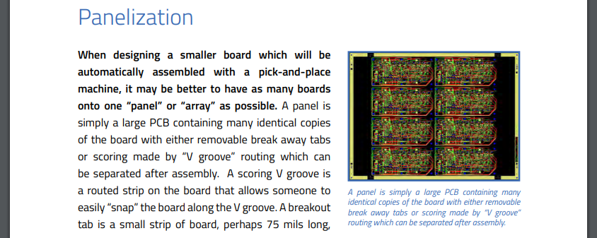
![]()